Exotic ST12-Gemanium - Dr. Duckyoung Kim
JANUARY. 03, 2017
Scientists at Geophysical Lab, Yanshan University and HPSTAR combined experimental and theoretical methods to probe the exotic properties of one special form-ST12-Ge of the element germanium. The results solve the long-standing debate on the optical and electronic properties of semiconducting Ge and suggest ST12-Ge to be a better material for infrared detection and imaging instead of single-junction solar absorbing.
Germanium as a frequently studied element in IVa element group, has the applications for next-generation computer architecture as well as implications for fundamental condensed matter physics. Germanium is used in fiber-optic systems, specialized camera and microscope lenses, circuitry, and solar cells. It is also an attractive anode material for lithium-ion batteries because it has a large theoretical charge-discharge capacity compared to graphite as well as high lithium ion diffusivity at room temperature compared to silicon.
ST12 phase for Germanium comes from its simple tetragonal structure containing 12 atoms per unit cell, resulting from slow decompression process. ST12-Ge was first observed about six decades ago, attracting both theoretical and experimental studies as a great solar absorber candidate. However, great controversies exist about its electronic structure and thermal stability due to lack of bulk pure sample.
New research published in Nature Communications (doi:10.1038/ncomms13909) from an international team Geophysical Laboratory, Yanshan Universtiy and HPSTAR, of scientists describe their work probing intrinsic semiconductor properties of bulk (~2 mm in diameter) ST12-Ge, a metastable phase of element gemanium.
“Bulk pure sample will allow for more accurate and concise electrical and optical measurements,” said Dr. Zhao, 啊lead author of the study. “However, the intrinsic properties have never been realized in ST12-Ge because the samples obtained in previous studies were either impure or too small to probe their practical performance.”
To synthesize bulk ST12-Ge, the researchers utilized a large volume high-pressure facility called multi-anvil press. To get ST12-Ge, they slowly decompressed the sample from 14 gigapascals at room temperature according to kinetic origins. ~15 mg (~2mm in diameter and length) recovered pellets were then polished for the following serials of measurements.
Bulk ST12-Ge shows both very small so-called "indirect electronic band gap", meaning that light is easily absorbed or emitted. and "direct band gap" meaning that it is much more difficult to absorb or emit light. “The smaller band gaps suggest ST12-Ge could be a good candidate for infrared detection, imaging and high-frequency and low-voltage electronic applications.” said Dr. Zhao. “Our work solves the long-standing debate regarding the band structure of ST12-Ge,”
 “Future research is required to understand its structure conversion pathways, but the result of this study, experimental and theoretical, pinpoint a clear picture of the intrinsic properties of ST12-Ge, added Dr. Kim, a co-author of the study who carry out the theoretical calculation of the work and also a staff scientist of HPSTAR.
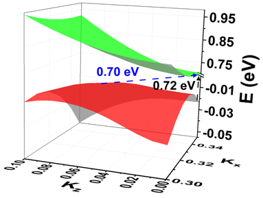
Caption: A schematic diagram of the valence and conduction bands. It is worth noting that the fundamental indirect gap is not along a high-symmetry direction.
锗作为典型的IVA族元素具有丰富的结构多样性。常温常压条件下,锗以金刚石结构存在,是当今最常见的一种半导体材料。当室温压缩金刚石结构的锗时,它将在10GPa的压力之上转变成金属性的四方β-锡结构的高密度锗。然而这种相变呈现不可逆性,在缓慢的降压过程中,β-锡结构的锗将转变成动力学上更稳定的另一种简单四方结构的亚稳锗(ST12-Ge)。对于ST12锗,过去人们较多的关注于其相变机理的研究,对其能带结构及光学的研究虽然也有不少的理论和实验报道,但是由于前人在样品制备方面的局限性以及理论预测的差异,因此对其能带结构和光学特性一直以来都存在着很大的争议。本工作中,当前的研究团队通过大腔体压机合成了毫米级别、纯相的锗多晶块材,并通过X射线衍射、透射电镜、拉曼光谱等确定了其晶体结构。光学和电输运测试结果表明ST12锗是一种半导体材料,具有间接带隙0.59eV和直接带隙0.74eV,这与他们的第一性原理计算结果相吻合。与常见的金刚石结构的锗相比,ST12锗具有更小的带隙,这意味着ST12锗可以更佳的应用于红外光学器件中。本研究结束了50多年以来对ST12锗电子结构和光学特性的长期争论。
