Pressure-gated band-edge states of 2D halide perovskites - Dr. Xujie Lü
NOVEMBER 3, 2022
In For semiconductor heterostructures, reconfiguring the band-edge states and modulating their interplay with charge carriers in a continuous manner have been a long-standing challenge. Recently, an international research team led by Dr. Xujie Lü from the Center for High Pressure Science and Technology Advanced Research (HPSTAR) and Prof. Letian Dou from Purdue University chosen the organic semiconductor-incorporated 2D halide perovskites as a model system. and They discovered that lattice compression induces induced band-alignment switching and charge redistribution, which giving realized controllable emission properties of these 2D hybrid semiconductor heterostructures. The work, entitled “Reconfiguring band-edge states and charge distribution of organic semiconductor-incorporated 2D perovskites via pressure gating", is published in Science Advances.
Two-dimensional (2D) semiconductor heterostructures are key building blocks for many electronic and optoelectronic devices. Fundamental questions remain regarding the effects of the interfacial band states on the carrier dynamics and optoelectronic properties, which is limited by the scarcity of suitable material systems as well as the difficulty in continuously tuning the frontier electronic structures via conventional methods.” said by Dr. Lü. “To this end, we proposed a new strategy and realized the manipulation of band-edge states and charge distribution via mechanical – rather than chemical or thermal – regulation.”

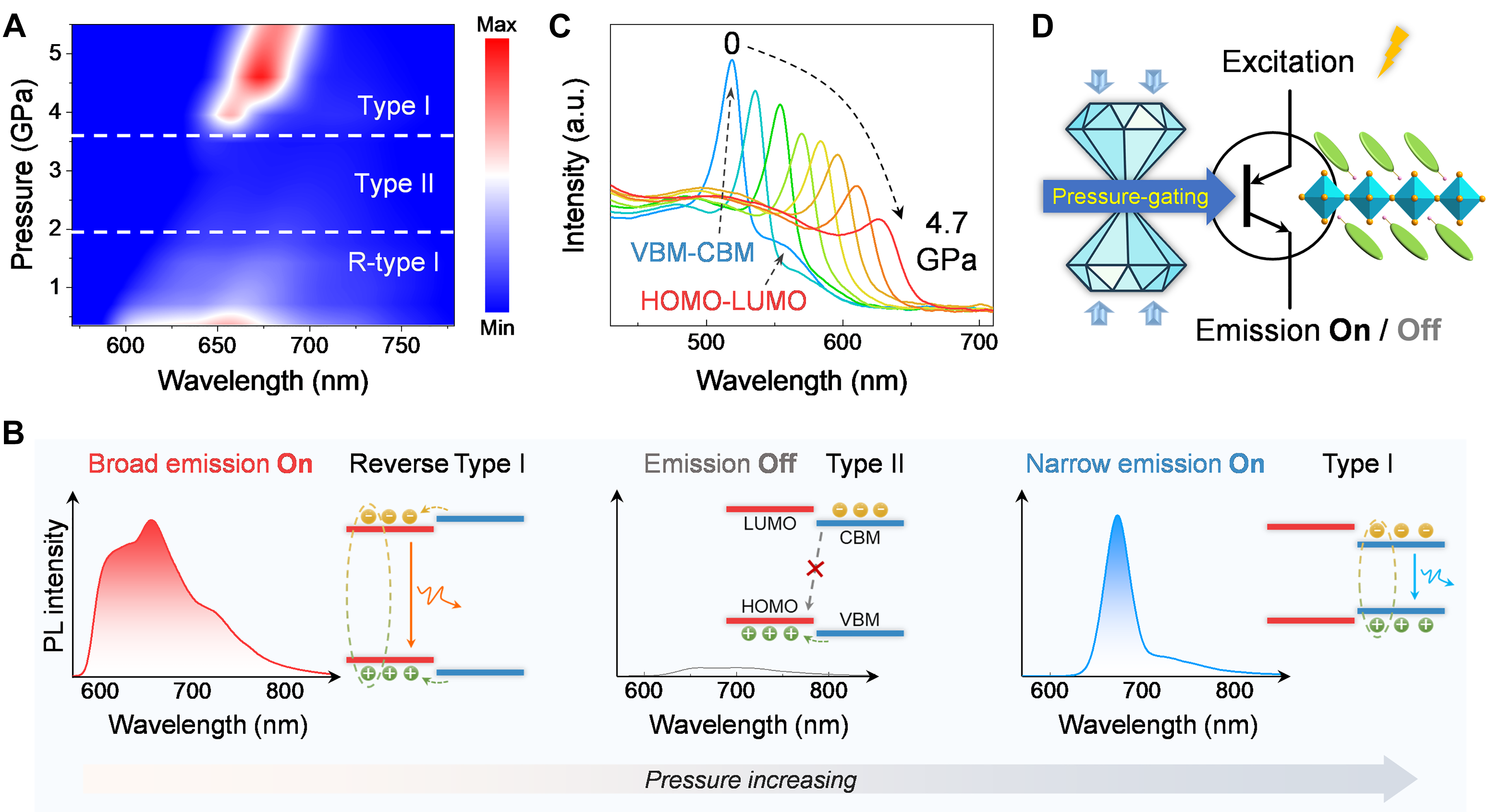
Figure 1. Pressure-controlled multiple emission states in 2D hybrid perovskite (BTm)2PbI4.
By continuously regulating the energy levels of organic and inorganic building blocks of organic semiconductor-incorporated 2D halide perovskites using external pressure, the researchers have demonstrated the possibility to fine-tune the band-edge states and the charge distribution of the 2D semiconductor heterostructures previously unattainable. “The band-alignment transition at the organic-inorganic interface is intrinsically not well-resolved at room temperature owing to the thermally-activated transfer and shuffling of band-edge carriers.” explained by Songhao Guo, a Ph.D. student at HPSTAR. The researchers have also proposed a “pressure-gating” strategy that enables the control of multiple emission states within a single material. This work provides important fundamental insights into the energetics and carrier dynamics of hybrid semiconductor heterostructures.
二维杂化半导体异质结是电子和光电器件的重要组成部分,通过调制有机和无机组分及其界面相互作用,可以实现在分子水平上对其电子结构和光电特性的设计。如何连续调节半导体异质结的带边电子态并实现界面处电荷分布的调控是一个长期存在的挑战。为此,由北京高压科学研究中心(HPSTAR)吕旭杰研究员和美国普渡大学Letian Dou教授领导的国际研究团队以有机半导体结合的二维卤化物钙钛矿为研究对象,通过压力调控实现了二维杂化半导体异质结电荷分布的连续调节和带边电子态的重构。他们利用二维钙钛矿中有机和无机组成单元在压力下不同的响应速度,通过压力来精细调控材料的带边状态,从而实现对其光电特性的调制和优化。此外,该研究还首次提出并论证了一种“压力门控”策略,可以在单一材料中实现压力驱动的多种发光状态转变。相关成果以“Reconfiguring band-edge states and charge distribution of organic semiconductor-incorporated 2D perovskites via pressure gating”为题,发表于近期的《Science Advances》上。
