Opening up the Bandgap of Graphene - Dr. Feng Ke
APRIL 20, 2019
A team of scientists led by Dr. Feng Ke of HPSTAR observed the semiconducting character in compressed trilayer graphene through in-situ electrical measurements. An intrinsic bandgap of ~2.5 eV has been achieved. The realization of such wide bandgap in graphene opens new opportunities in carbon-based electronic devices. Their study was published in the recent issue of PNAS.
Graphene, the two-dimensional form of carbon, its extraordinary electron mobility and super thin structure makes it appealing for substituting silicon in future electronic devices. However, one big problem or challenge for graphene is its zero bandgap—impossible on/off field effect transition and a low on/off transistor switching ratio. This means that graphene's electron conduction can't be completely cut off, while it is an essential requirement for on/off devices.
'The small bandgap has been greatly limited graphene’s applications in electronic and photonic devices because we are not able to modulate the electron conduction,' said Dr. Feng Ke, the lead author of the study. 'Thus opening and finally controlling the bandgap in graphene are thelongstanding goals.'
Considerable efforts have been made to open the bandgap of graphene, using quantum confinement by patterning graphene in the form of a quantum dot, nanoribbon, and nanomesh, or symmetric breaking and selective control of the carrier concentration in graphene layers by an external electric field. While only several hundred meV bandgap was reached in bilayer graphene, still far below the threshold for practical applications.
A research team led by HPSTAR scientists in collaboration with University of California, Berkeley have been able to open an intrinsic bandgap of 2.5±0.3 eV in trilayer graphene by applying external pressure.
“The pressure tuned the interlayer interaction between graphene layers”, explained Dr. Feng Ke.
Dr. Ke and his colleagues made two key processes that led to the successful opening of a large bandgap in trilayer graphene. The first was the newly developed lithography technique of microelectrode fabrication. “This ensures the good contact between the film samples and hand-wired electrodes, which thus greatly improved the stability of electrodes under compression,” explained Dr. Feng Ke.
Based on this new technique, they conducted the in-situ high-pressure electrical measurements up to 60 GPa and observed the semimetallic-semiconducting transition in trilayer graphene.
The optical absorption measurements demonstrated that an intrinsic bandgap of 2.5±0.3 eV could be achieved in such a semiconducting state, and could be preserved to very low pressure.
“Our study removes the doubt on the realization of large intrinsic bandgap in few-layer graphene”, said Dr. Bin Chen, one of the corresponding author. “The explorations for the practical applications of graphene-based electronic devices could be really stimulated after this realization of large bandgap in graphene”.
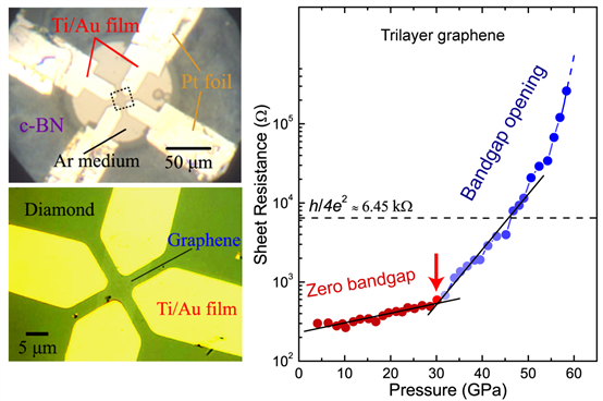
Caption: Top left: A perspective view of the designed microwiring setup. Bottom left: Top view of the trilayer graphene sample and probing electrodes in a diamond anvil cell. Right: Resistance–pressure curves of trilayer graphene measured at room temperature (300 K).
石墨烯的发现获得了2010年诺贝尔物理奖, 从此厚载众望, 盼将取代硅基半导体, 引发新一轮科技革命。然而,科学家们经过多年的努力,才将石墨烯的零带隙打开至0.3eV,远远低于应用要求。来自北京高压科学中心的科学家与其合者运用压力调控层间相互作用,成功将三层石墨烯的带隙打开至2.5±0.3eV。们通过实验技术探索与创新,运用光刻技术制备薄膜电极保证样品与电极间的良好接触,结合手工布线和传压介质技术保证电极在极端高压环境下的稳定性。首次实现了超高压力下对只有几层厚度薄膜样品进行原位电输运性质测量—电学测量是判断材料金属-绝缘体转变以及带隙打开的直接证据。使用光刻技术制备薄膜电极是我们高压下的薄膜材料电学测量的关键。